
Service | Messages
-

Product Center
-

Applications
Henan Wanmo Diamond(Wanmo Diamond) is a comprehensive technology-oriented enterprise specializing in high-end superhard materials.The company's main business includes customized metal bond diamonds and various types of diamon
-

About us
Henan Wanmo Diamond(Wanmo Diamond) is a comprehensive technology-oriented enterprise specializing in high-end superhard materials.The company's main business includes customized metal bond diamonds and various types of diamon

Commercial Acceleration of Diamond Semiconductor
Time:
2023-08-21
On August 2, scientists at Chiba University in Japan announced that they have developed a method of manufacturing diamond wafers using lasers, which is expected to power the next generation of semiconductors.
Although silicon is still the main material of semiconductors, the wide band gap of gallium nitride and silicon carbide enables semiconductor materials to function more effectively at higher voltages, frequencies and temperatures. With the acceleration of the adoption of electric vehicles, the demand for wide band gap silicon carbide components is also increasing.
Compared with silicon carbide, diamond has a higher band gap (up to 5.45 eV). Its greatest advantages lie in higher carrier mobility (hole: 3800 cm2V-1s-1, electron: 4500 cm 2 V-1s-1), higher breakdown electric field (>10 MVcm-1) and higher thermal conductivity (22 WK-1cm-1). Its intrinsic material advantage is that it has the highest thermal conductivity in nature and the highest mobility of bulk materials, it can meet the needs of high power, strong electric field and radiation resistance in the future, and is an ideal material for the production of power semiconductor devices. It has broad application prospects in smart grid, rail transit and other fields.
However, at present, there is still a large distance for the commercial application of diamond. The high cost and small size of diamond materials are the main obstacles to the development of diamond power electronics. For example, the dislocation density of nitrogen-doped diamond single crystal flakes (6mm × 7mm) prepared by CVD can currently be as low as 400 cm-2. However, when the wafer of diamond heteroepitaxial technology reaches 4-8 inches, the dislocation density is still as high as the order of 107 cm-2, and the high defect density is still a challenge.
More importantly, diamond is still brittle and difficult to process. Although the hardness of diamond is very high, when it breaks, they break in very specific irregular ways, which is very challenging for manufacturing semiconductor wafers.
Recently, a research team led by Professor Hidai, Hirofumi of the Graduate School of Engineering at Chiba University in Japan, found a way to solve this problem. They used a novel laser-based slicing technique that can be used to cleanly cut diamonds along optimal crystal planes to produce smooth wafers. Their work is detailed in an article published in the journal Diamond and Related Materials.
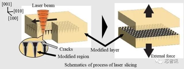
The properties of most crystals, including diamond, vary along different crystal planes, which are imaginary surfaces containing the atoms that make up the crystal. For example, a diamond can be easily cut along the {111} surface. However, cutting {100} is challenging because it also creates cracks along the {111} cleavage plane, increasing kerf loss.
To prevent these unwanted crack propagation, the researchers developed a diamond machining technique that focuses short laser pulses on a narrow, conical volume within the material. Professor Hidai explained that concentrated laser irradiation converts diamond into amorphous carbon with a lower density than diamond. Therefore, the density of the area modified by the laser pulse decreases and cracks can form.
By shining these laser pulses in a square grid pattern onto a transparent diamond sample, the researchers created a grid of small crack-prone areas inside the material. If the space between the modified regions in the grid and the number of laser pulses used per region are optimal, then all modified regions are interconnected by small cracks that preferentially propagate along the {100} plane. Therefore, a smooth wafer with a {100} surface can be easily separated from the rest of the block by simply pushing a sharp tungsten needle to the side of the sample.
Overall, this technology is a key step in making diamond a next-generation semiconductor material. In this regard, Professor Hidai said that diamond cutting can produce high-quality wafers at low cost and is indispensable for the manufacture of diamond semiconductor devices. Therefore, this research brings us closer to realizing various applications of diamond semiconductors in society, such as improving the power conversion rate of electric vehicles and trains.
Hidai and Chiba University are not the only institutions looking to harness diamonds to power the next generation of computing and communications technology.
In September 2021, AKHAN Semiconductor (AKHAN Semiconductor) announced the manufacture of the world's first 300mm metal-oxide complementary semiconductor (CMOS) diamond wafer. According to reports, this new technology will improve the power handling, thermal management and durability of electronic products in various industries and manufacturing processes.
In April, Amazon Web Services partnered with De Beers subsidiary Element Six to develop synthetic diamonds for quantum key distribution. The idea is to engineer defects (called color cores) in the diamond that can absorb photons containing quantum information and then re-emit them. Amazon hopes to use this phenomenon to create repeaters that can extend the reach of quantum key distribution to its global network.
In an earlier interview, Antia Lamas-Linares, head of the AWS Quantum Network Center, said that the quantum network is only a few years away from completion.
Recommended content
Share to

Innovative Technology, Strict Quality Control
Contact us
Telephone:+86-0371-6239 0096
Email:info@wanmodia.com
Address:Intersection of Wanhong RD. & Hefeng Str., Zhongmu, Zhengzhou, Henan
Copyright © Henan Wanmo Diamond Co., LTD.
SAF Coolest v1.1 设置面板 IOZSX-ZPHF-TDAWE-AXV
无数据提示
Sorry, there is no information in the current column!