
Service | Messages
-

Product Center
-

Applications
Henan Wanmo Diamond(Wanmo Diamond) is a comprehensive technology-oriented enterprise specializing in high-end superhard materials.The company's main business includes customized metal bond diamonds and various types of diamon
-

About us
Henan Wanmo Diamond(Wanmo Diamond) is a comprehensive technology-oriented enterprise specializing in high-end superhard materials.The company's main business includes customized metal bond diamonds and various types of diamon

Major Breakthrough in Diamond Semiconductor Laser Cutting Technology
Time:
2023-08-07
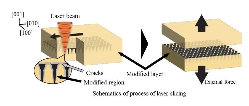
On Tuesday, local time, the official website of Chiba University in Japan announced that a research team led by Professor Hidai, Hirofumi of the Graduate School of Engineering of the school, found a solution to this problem. They used a new laser dicing technique that uses laser pulses to cut diamond into thin slices, claiming to "pave the way for the next generation of semiconductor materials". It can be used to cleanly cut diamonds along optimal crystal planes to produce smooth wafers.

With the upgrading of the global semiconductor market, China's domestic equipment manufacturers also ushered in new development opportunities. As the core field of localization, semiconductor equipment is of great significance to the security of China's semiconductor industry chain. In recent years, under the influence of multiple factors, the speed of verification and import of local equipment manufacturers is also accelerating. Among them, the field of "cutting" has become one of the highlights. Especially wafer cutting, the development of laser will further help China's semiconductor localization process.
Article source IT home, global cutting-edge science and network information, China superhard materials network comprehensive finishing.
Recommended content
Share to

Innovative Technology, Strict Quality Control
Contact us
Telephone:+86-0371-6239 0096
Email:info@wanmodia.com
Address:Intersection of Wanhong RD. & Hefeng Str., Zhongmu, Zhengzhou, Henan
Copyright © Henan Wanmo Diamond Co., LTD.
SAF Coolest v1.1 设置面板 IOZSX-ZPHF-TDAWE-AXV
无数据提示
Sorry, there is no information in the current column!